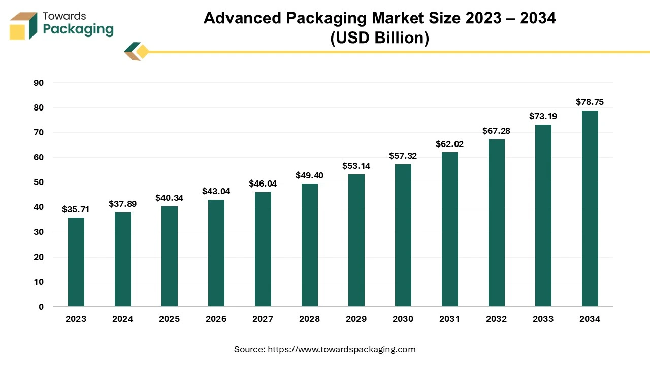
Ottawa, Dec. 15, 2025 (GLOBE NEWSWIRE) -- The global advanced packaging market reported a value of USD 40.34 billion in 2025, and according to estimates, it will reach USD 78.75 billion by 2034, as outlined in a study from Towards Packaging, a sister firm of Precedence Research.
The advanced packaging market is growing rapidly as industries demand higher chip performance, miniaturization, and energy efficiency. North America remains the dominant region due to its strong semiconductor ecosystem, rapid adoption of AI and 5G technologies, and continuous R&D investments. Rising use of 2.5D/3D packaging, fan-out solutions, and wafer-level technologies further strengthens the region’s technological leadership.
Request Research Report Built Around Your Goals: sales@towardspackaging.com
What is meant by advanced packaging market?
Advanced packaging refers to next-generation semiconductor packaging technologies designed to improve chip performance, efficiency, miniaturization, and integration. It includes 2.5D/3D integration, fan-out packaging, system-in-package (SiP), and wafer-level packaging techniques that enable faster processing, higher bandwidth, and better thermal management. Driven by rising demand for high-performance computing, AI, 5G devices, electric vehicles, and compact consumer electronics, the advanced packaging market continues to expand as industries seek solutions that combine functionality, speed, and lower power consumption.
What Are the Latest Key Trends in the advanced packaging market?
- Rise of 2.5D/3D and 3D-stacked packaging (chiplet & heterogeneous integration) — Packaging is moving beyond flat monolithic chips: by stacking dies or combining various modules (CPU, memory, I/O) in one package (2.5D/3D or “chiplets”), manufacturers squeeze more performance, density and energy-efficiency into smaller footprints.
- Hybrid bonding & finer interconnects — New bonding techniques (e.g. hybrid bonding) enable ultra-fine interconnect pitch (micrometer-scale), boosting bandwidth and lowering latency. This supports high-bandwidth memory (HBM) stacks and AI/data-center workloads needing dense connections.
- Fan-out wafer-level packaging (FOWLP) and compact package growth — Fan-out WLP and similar wafer-level techniques are increasingly used to build thinner, smaller packages useful for mobile, wearable, IoT, and other space-constrained devices where compactness + performance matters.
- Panel-level packaging (PLP) & scalable manufacturing — Use of larger panel substrates (rather than individual wafers) is rising, which can lower per-unit cost and improve throughput attractive as demand for high-volume, high-performance chips (e.g. for AI, telecom, automotive) scales up.
- Growing demand from AI, HPC, automotive & 5G/telecom sectors — Chips for AI accelerators, data centers, autonomous vehicles and 5G infrastructure need high-bandwidth, high-performance packaging. This growing demand is pushing adoption of advanced packaging as a core enabler, not just a niche option.
- Material Innovation and Sustainability Focus — Advanced substrates (organic, ceramic, novel interconnect materials) along with efforts to improve thermal management, reliability, and possibly more sustainable manufacturing practices are gaining attention as packaging complexity increases.
What is the Potential Growth Rate of the Advanced Packaging Market?
Rising Demand for Data-center Chips
The rising demand for AI, HPC, and data-center chips is accelerating the need for high-performance, low-latency, and thermally efficient architectures, pushing manufacturers toward 2.5D, 3D, and chiplet-based advanced packaging. At the same time, the miniaturization of smartphones, wearables, and IoT devices requires thinner, compact, and power-efficient components. Together, these trends drive strong adoption of advanced packaging solutions that enhance density, bandwidth, and energy efficiency while enabling smaller, more powerful next-generation electronics.
More Insights of Towards Packaging:
Regional Analysis:
- MEA Flexible Packaging Market Size, Trends, Key Segments, and Regional Dynamics with Manufacturers and Suppliers Data
- Asia Pacific Flexible Plastic Packaging Market Size, Trends, Segments, Companies, Competitive Analysis, Value Chain & Trade Analysis 2025-2035
- U.S. Rigid Packaging Market Size, Trends, Key Segments, and Dynamics with Manufacturers and Suppliers Data
- High-Barrier Packaging Films Market Size, Trends, Segments, Companies, Competitive Analysis, Value Chain & Trade Analysis 2025-2035
- Europe Cigarette Packaging Market Size, Trends, Segments, Competitive Landscape Report
- Converted Flexible Packaging Market Size, Trends, Segments, Regional Outlook (NA, EU, APAC, LA, MEA), Competitive Landscape, Value Chain and Trade Analysis
- Compostable Tableware Market Size, Trends, Segments, Regional Outlook, Competitive Landscape & Trade Analysis 2025-2035
- RFID Smart Packaging Market Size, Trends, Segmentation, Regional Outlook (NA, EU, APAC, LA, MEA), Competitive Landscape, and Trade & Value Chain Analysis
- Sustainable Minimalistic Tableware Packaging Market Size, Trends, Segments, Regional Outlook (NA, EU, APAC, LA, MEA), Competitive Analysis, Value Chain & Trade Insights
- Mono-Material Barrier Packaging Market Size, Trends, Segments, Regional Insights, Competitive Analysis, and Global Trade Data 2025-2034
- Stretch Wrap Packaging Market Size, Trends, Segments, Regional Insights (NA, EU, APAC, LA, MEA), Leading Companies, and Competitive Landscape Analysis 2025–2034
- Trigger Spray Bottle Market Size, Regional Outlook (NA, EU, APAC), Segments, Competitors, Value Chain and Trade Analysis, 2025-2035
- Integrated Circuit Packaging Market Size, Trends, Segments, Regional Outlook (NA, EU, APAC, LA, MEA), Competition, Value Chain & Trade Analysis 2025-2035
- Temperature Controlled Packaging Solutions Market Size, Trends, Segments Data, Regional Outlook (NA, EU, APAC, LA, MEA) Value Chain Analysis 2025-2034
- Biodegradable Cutlery Market Size, Trends, Segments, Regional Outlook (NA, EU, APAC, LA, MEA), Competitive Landscape, Value Chain and Trade Analysis 2025-2035
Who is the Leader in Advanced Packaging Market?
North America dominates the advanced packaging market due to its strong semiconductor ecosystem, early adoption of AI, HPC, and data-center technologies, and the presence of major chipmakers and OSAT innovators. Significant R&D investments, robust government support for onshore chip manufacturing, and high demand from automotive, aerospace, telecom, and consumer electronics industries further strengthen the region’s leadership in advanced packaging technologies.
What are the Ongoing Trends in the U.S. Market?
The U.S. dominates the North America market due to its strong semiconductor manufacturing base, leadership in AI and HPC chip development, and high investments in advanced packaging R&D. Robust government funding, presence of leading tech companies, and strong demand from data centers, aerospace, and automotive sectors further strengthen its position.
How is the Opportunistic is the Rise of the Asia Pacific in the Advanced Packaging Market?
Asia-Pacific is the fastest-growing region in the advanced packaging market due to its strong semiconductor manufacturing ecosystem, expanding electronics production, and rapid adoption of AI, 5G, and automotive technologies. Countries like China, Taiwan, South Korea, and Japan invest heavily in chip fabrication, wafer-level packaging, and heterogeneous integration, while growing consumer electronics and EV demand further accelerate regional market expansion.
What are the Ongoing Trends in the China Market?
China dominates the market due to its extensive semiconductor manufacturing base, strong government support, and rapidly expanding electronics and AI industries. The country invests heavily in wafer-level packaging, 2.5D/3D integration, and panel-level technologies, supported by large domestic demand from smartphones, consumer electronics, automotive, and telecom sectors. Its strong supply chain and skilled workforce further reinforce its leadership.
How Big is the Success of the Europe Advanced Packaging Market?
Europe is growing at a notable rate in the market due to rising investments in semiconductor manufacturing, strong demand from automotive, industrial automation, and aerospace sectors, and increasing adoption of AI, 5G, and IoT technologies. Government initiatives to enhance chip production, along with advancements in heterogeneous integration and wafer-level packaging, further accelerate regional market expansion.
What are the Ongoing Trends in U.K. Market?
The UK is a dominant country in Europe’s advanced packaging market due to its strong semiconductor R&D capabilities, leadership in chip design, and growing adoption of AI, quantum computing, and automotive electronics. Significant government funding, expanding collaborations with global packaging firms, and increasing demand for high-performance, energy-efficient devices support the country’s steady advancement in advanced packaging technologies.
How Crucial is the Role of Latin America in Advanced Packaging Market?
Latin America is growing at a considerable rate in the advanced packaging market due to increasing adoption of smartphones, consumer electronics, and automotive technologies, especially EVs. Expanding telecom infrastructure, rising investments in semiconductor assembly, and growing interest in IoT and industrial automation support market growth. Government initiatives to strengthen electronics manufacturing further enhance the region’s advancement.
How Big is the Opportunity for the Growth of the Middle East and Africa Advanced Packaging Market?
The Middle East and Africa hold a growing opportunity in the market driven by expanding telecom networks, rising adoption of AI, IoT, and smart infrastructure, and increasing demand for high-performance electronics. Government-led digitalization programs and emerging semiconductor assembly investments further strengthen the region’s potential for future growth.
Elevate your packaging strategy with Towards Packaging. Enhance efficiency and achieve superior results - schedule a call today: https://www.towardspackaging.com/schedule-meeting
Segment Outlook
Packaging Platform Insights
What made the Flip Chip Segment Dominant in the Advanced Packaging Market in 2024?
The flip-chip segment is dominant in the market because it delivers superior electrical performance, higher I/O density, and excellent thermal dissipation compared to traditional wire bonding. Its ability to support high-speed, high-performance chips used in AI, HPC, 5G, and advanced consumer electronics makes it the preferred packaging solution across major industries.
The embedded-dies segment is the fastest-growing in the market because it enables ultra-thin, compact, and lightweight designs ideal for wearables, IoT devices, and miniaturized electronics. It offers shorter interconnects, improved signal integrity, and better thermal performance. Its ability to integrate multiple functions within substrates drives strong adoption in automotive, medical, and high-performance applications.
End-Use Industry Insights
How the Consumer Electronics Dominated the Advanced Packaging Market in 2024?
The consumer electronics segment dominates the market due to the high demand for smartphones, tablets, wearables, and smart devices requiring compact, high-performance, and energy-efficient chips. Advanced packaging solutions, such as flip-chip and fan-out wafer-level technologies, enhance device functionality, thermal management, and reliability, driving widespread adoption in this segment.
The automotive segment is the fastest-growing in the market due to increasing adoption of electric vehicles, autonomous driving systems, and advanced driver-assistance systems (ADAS). These technologies require high-performance, reliable, and thermally efficient chips, driving demand for 2.5D/3D packaging, embedded-die solutions, and other advanced semiconductor packaging innovations.
Join now to access the latest packaging in industry segmentation insights with our Annual Membership: https://www.towardspackaging.com/get-an-annual-membership
Recent Breakthroughs in Advanced Packaging Market
- In February 2025, ASMPT introduced a new “next‑gen wire bonder” (AERO PRO), designed for high-density IC packaging and enabling more precise, fine-pitch wire bonding. Furthermore, in March 2025, ASMPT unveiled its “CamSpector PRO” inspection tool for CMOS image‑sensor packaging, delivering advanced flaw detection to improve yield and packaging quality. Moreover, in April 2025, ASMPT announced an enhanced version “AERO PRO XPOWER 2.0,” further improving wire‑bonding accuracy and efficiency in advanced packaging production.
- In September 2025, During SEMICON West 2025, ASMPT unveiled a full advanced‑packaging portfolio: including a thermo‑compression bonding system (FIREBIRD AOR TCB), the ALSI LASER1206 automatic dicing system, AMICRA NANO precision die attach tool, NEXX Stratus™ P500 panel‑plating system, and hybrid SIPLACE CA2 targeting dense 2.5D/3D‑IC and AI/HPC chip packaging.
Top Companies in the Global Advanced Packaging Market
- ASE Technology Holding Co. Ltd.
- Amkor Technology
- Taiwan Semiconductor Manufacturing Company (TSMC)
- Intel Corporation
- Samsung Electronics Co. Ltd.
- Jiangsu Changjiang Electronics Technology Co. Ltd. (JCET)
- Siliconware Precision Industries Co. Ltd. (SPIL)
- Powertech Technology Inc.
- STATS ChipPAC Pte. Ltd.
- ChipMOS Technologies Inc.
- Fujitsu Semiconductor Ltd.
- Texas Instruments
- Analog Devices
- Deca Technologies
- HANA Micron Inc.
Global Advanced Packaging Market Segments
By Packaging Platform
- Flip Chip
- Fan-in WLP
- Fan-out
- Embedded Die
- 2.5D/3D
By End-Use Industry
- Consumer Electronics
- Automotive
- Telecommunications
- Healthcare
- Industrial
- Others
By Region
- North America:
- U.S.
- Canada
- Mexico
- Rest of North America
- South America:
- Brazil
- Argentina
- Rest of South America
- Europe:
- Western Europe
- Germany
- Italy
- France
- Netherlands
- Spain
- Portugal
- Belgium
- Ireland
- UK
- Iceland
- Switzerland
- Poland
- Rest of Western Europe
- Eastern Europe
- Austria
- Russia & Belarus
- Türkiye
- Albania
- Rest of Eastern Europe
- Asia Pacific:
- China
- Taiwan
- India
- Japan
- Australia and New Zealand,
- ASEAN Countries (Singapore, Malaysia)
- South Korea
- Rest of APAC
- MEA:
- GCC Countries
- Saudi Arabia
- United Arab Emirates (UAE)
- Qatar
- Kuwait
- Oman
- Bahrain
- South Africa
- Egypt
- Rest of MEA
Invest in Our Premium Strategic Solution: https://www.towardspackaging.com/checkout/5390
Request Research Report Built Around Your Goals: sales@towardspackaging.com
About Us
Towards Packaging is a global consulting and market intelligence firm specializing in strategic research across key packaging segments including sustainable, flexible, smart, biodegradable, and recycled packaging. We empower businesses with actionable insights, trend analysis, and data-driven strategies. Our experienced consultants use advanced research methodologies to help companies of all sizes navigate market shifts, identify growth opportunities, and stay competitive in the global packaging industry.
Stay Connected with Towards Packaging:
- Find us on Social Platforms: LinkedIn | Twitter | Instagram | Threads
- Subscribe to Our Newsletter: Towards Sustainable Packaging
- Visit Towards Packaging for In-depth Market Insights: Towards Packaging
- Read Our Printed Chronicle: Packaging Web Wire
- Get ahead of the trends – follow us for exclusive insights and industry updates:
Pinterest | Medium | Tumblr | Hashnode | Bloglovin | LinkedIn – Packaging Web Wire | Globbook | Substack | Bluesky | - Contact: APAC: +91 9356 9282 04 | Europe: +44 778 256 0738 | North America: +1 8044 4193 44
Our Trusted Data Partners
Precedence Research | Statifacts | Towards Healthcare | Towards Auto | Towards Food and Beverages | Towards Chemical and Materials | Towards Consumer Goods | Towards Dental | Towards EV Solutions | Nova One Advisor | Healthcare Webwire | Packaging Webwire | Automotive Webwire | Nutraceuticals Func Foods | Onco Quant | Sustainability Quant | Specialty Chemicals Analytics
Towards Packaging Releases Its Latest Insight - Check It Out:
- Clarified Polypropylene Bottles Market Size, Trends, Segments, Regional Outlook (NA, EU, APAC, LATAM, MEA), Competitive Analysis, Manufacturers and Trade Data
- Sustainable Pharmaceutical Packaging Market Size, Trends, Segments, Regional Insights, and Competitive Landscape 2025-2034
- Mono-material Plastic Packaging Film Market Size, Trends, Segmentation, and Competitive Landscape 2025-2034
- Shipping Labels Market Size, Trends, Segments, Regional Insights, and Competitive Landscape Analysis 2025-2034
- Metallized Rollstock Film Market Size, Share, Trends & Forecast 2025-2035
- IBC Tanks Market Size, Share, Trends, Regional Analysis, and Competitive Landscape 2025-2034
- Packaging Inks and Coatings Market Size, Trends, Regional Insights, and Competitive Landscape 2025-2034
- U.S. Vacuum Sealer Bags Market Size, Trends, Segmentation and Competitive Landscape 2025-2034
- Sterile Medical Paper Packaging Market Size, Trends, Segmentation, Regional Outlook (NA, EU, APAC, LA, MEA), Competitive Landscape & Trade Analysis
- Australia Vacuum Sealer Bags Market Size, Trends, Segments, Competition & Trade Analysis
- Dog Food Container Market Size, Trends, Segments, Regional Outlook (NA, EU, APAC, LA, MEA), Competitive Landscape, and Trade & Supply Chain Insights
- Reusable Water Bottles Market Size, Share, Trends, Segments and Forecast 2035
- North America Insulated Packaging Market Size, Trends, Segments, Regional Insights, and Competitive Landscape 2025-2034
- Bioengineered Packaging Market Size, Trends, Segments, Regional Insights, and Competitive Landscape 2025-2034
- U.S. Custom Cardboard Boxes Market Size, Trends, Segments, Regional Outlook, Competitive Landscape & Trade Intelligence Report
