TOKYO, JAPAN--(Marketwired - Dec 9, 2015) - Leading semiconductor test equipment supplier Advantest Corporation (
Many IoT-enabled electronic products receive information in analog form, then convert it into digital signals for transmission. This requires the use of integrated digital ICs. These semiconductors are extremely cost sensitive and the markets for them are highly competitive. In addition, digital ICs are used in a wide range of applications, many of which impose stringent safety and reliability standards that put a premium on device performance and accuracy. For these reasons, producers of digital ICs typically employ high-mix, low-volume production methods, which require highly versatile and cost-efficient testing capabilities.
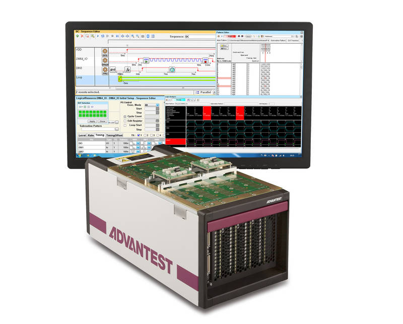
With its flexible architecture, the EVA100 Digital Solution can perform all of the functions needed for testing digital ICs as well as pattern generation and comparison for evaluating device designs, digital control, power source measurements and 18bit analog measurements. It can conduct all of these measurements at 100Mbps data-transfer rates and up 200MHz clock speeds, resulting in high-efficiency testing.
The EVA100 Digital Solution leverages the original platform's intuitive GUI which alleviates the need for users to know any high-level programming language. Like the other systems in the EVA100 product line, including the EVA100 Production Model introduced in November, the new system enables a customer to establish a common measurement environment throughout a facility, from design evaluation through production -- achieving efficiency-boosting standardization that is unmatched by any existing measurement instrument or system.
In addition, the EVA100 Digital Solution is 40 percent smaller than the initial EVA100 measurement system, saving time and money by simplifying operation and making periodic maintenance much easier. Scaling down the architecture also helps the EVA100 Digital Solution to deliver both high reliability and industry-leading productivity. With each compact unit having a maximum of 256 measurement channels, as many as four EVA100 Digital Solutions can be clustered together to create configurations of up to 1,024 digital channels. This enables the system to match manufacturing volumes with market needs by readily accommodating changes in production volumes and line retooling for different device types. It also gives users the flexibility to optimize test environments for logic circuits and IoT devices, many of which utilize DFT. Additionally, the measurement system can apply the same test programs for design and evaluation as for production, eliminating the need to change program codes and accelerating new devices' time to market.
"Widespread interest in IoT concepts and products, from automotive electronics to 'smart cities,' has led to increasing demand for electronic devices such as sensors," said Satoru Nagumo, managing executive officer at Advantest Corporation. "By expanding our EVA100 platform's capabilities to include testing of digital ICs, Advantest now offers this market segment the same optimized testing capabilities that other sectors enjoy."
About Advantest Corporation
A world-class technology company, Advantest is the leading producer of automatic test equipment (ATE) for the semiconductor industry and a premier manufacturer of measuring instruments used in the design and production of electronic instruments and systems. Its leading-edge systems and products are integrated into the most advanced semiconductor production lines in the world. The company also focuses on R&D for emerging markets that benefit from advancements in nanotech and terahertz technologies, and has introduced multi-vision metrology scanning electron microscopes essential to photomask manufacturing as well as groundbreaking 3D imaging and analysis tools. Founded in Tokyo in 1954, Advantest established its first subsidiary in 1982, in the USA, and now has subsidiaries worldwide. More information is available at www.advantest.com.
Contact Information:
Advantest Corporation
3061 Zanker Road
San Jose, CA 95134, USA
Judy Davies